Kavli nanolab

Kavli nanolab

Nanofabrication and characterization

Our nanofabrication and characterization services are primarily supported by the state-of-the-art equipment available at the Kavli Nanolab, a leading facility in the field. We utilize a wide range of advanced tools to deliver precise and innovative solutions tailored to your research and development needs. Below are the key pieces of equipment we rely on:

1- Raith EBPG5200 (Electron Beam Lithography System): This system enables the creation of ultra-precise nanoscale patterns on various substrates, making it ideal for high-resolution device fabrication and intricate nanostructures. 

2- EVG-620 (Mask Aligner): Used for photolithography, this aligner allows for the accurate transfer of patterns onto substrates through light exposure, essential for producing high-quality microelectronic and MEMS devices. 

3- μMLA Heidelberg Instruments (Laser Writer): Laser lithography is an advanced maskless lithography technique that enables the direct writing of patterns onto a substrate using a laser beam and without a physical mask. The μMLA laser writer uses a computer-controlled laser to create custom patterns, particularly useful for rapid prototyping, research, and small-scale production. 

1- Plassys MEB 550S (evaporation): is an advanced e-beam evaporation system for precise deposition of thin films, of “standard” materials including Ti, Pd, Nb, Al, AlOx, 

2- Temescal FC-2000 (evaporation) is a high-performance electron beam evaporation system designed for the deposition of thin films, particularly metals e.g. Ti, Al, Au, Ag, Pt, Cr. It is capable of depositing multiple materials in a single process, to achieve multilayered structures for advanced applications.

3- AC Dielectric Deposition System (sputter deposition): is used for depositing high-quality films through sputtering process. It is specifically designed to create thin dielectric layers, such as Si3N4, SiO2, HfO2, Al2O3, for applications in microelectronics and nanotechnology

4- AC Metal Deposition System (sputter deposition): is a sputtering tool used for depositing thin metal films, e.g. Cr, Mo, W, Co. It is designed for creating high-purity metal layers with precise control over thickness.

5- Super AJA Sputter System (sputter deposition): is an advanced tool for sputtering thin films of various metals and superconductors inclusiding NbTiN, Ta, Nb, Ti. It provides precise control over film thickness and composition.

6- FirstNano CVD Furnace (chemical vapor deposition): is a versatile chemical vapor deposition system used for the high-temperature annealing and the growth of high-quality thin films and nanomaterials, including carbon nanotubes and graphene.

7- Oxford PECVD System (PE-CVD): is a plasma-enhanced chemical vapor deposition tool used for depositing high-quality dielectric films, including SiO2, Si3N4 and SiC and a-Si.

1- Tepla 300 (plasma etching): The tool is used primarily for dry etching and surface cleaning of materials e.g. with O2 plasma. It is ideal for removing organic residues and preparing substrates for subsequent processing steps in nanofabrication and microelectronics. 

2- Oxford ICP Cl (reactive ion and plasma etching): The Oxford ICP-CL is an advanced dry etching tool used for high-precision etching processes in nanotechnology. It employs Inductively Coupled Plasma (ICP) technology to achieve fine feature etching on various substrates. The system is renowned for its exceptional etch uniformity, high etch rates, and ability to process complex patterns with great accuracy. It is a valuable asset for both research and industrial applications, offering reliable and repeatable results in the fabrication of nanostructures.

3- AMS 100 I-speeder (RIE plasma etching): Utilizing cryogenic temperatures, the AMS Cryo enables advanced etching of Si and SiN, with improved etch rates, selectivity, and feature resolution.

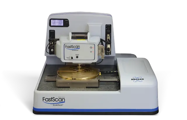
1- Bruker FastScan (AFM): The high-speed atomic force microscope delivers precise, high-resolution surface imaging at the nanoscale. Ideal for detailed surface analysis, providing valuable insights into sample topography and quality. 

2- Bruker Dektak XT (surface profilometer): is a fast solution for surface profiling and thickness measurements. It offers high-resolution, accurate data with a user-friendly interface. 

3- FEI NovaNanoSEM (Specimen surface inspection): is a cutting-edge scanning electron microscope designed for high-resolution imaging and analysis of nanostructures. With its advanced imaging capabilities and versatility, it provides detailed insights into sample morphology and surface features. 

4- Renishaw Invia Reflex (Raman spectroscopy): is a sophisticated analytical tool used for high-resolution chemical and structural analysis. It utilizes Raman spectroscopy to provide detailed information about molecular vibrations, enabling the identification and characterization of materials at the microscopic level.

5- Woollam M-2000 (ellipsometer): It provides detailed measurements of film thickness, refractive index, and optical properties of the materials and complex systems. 

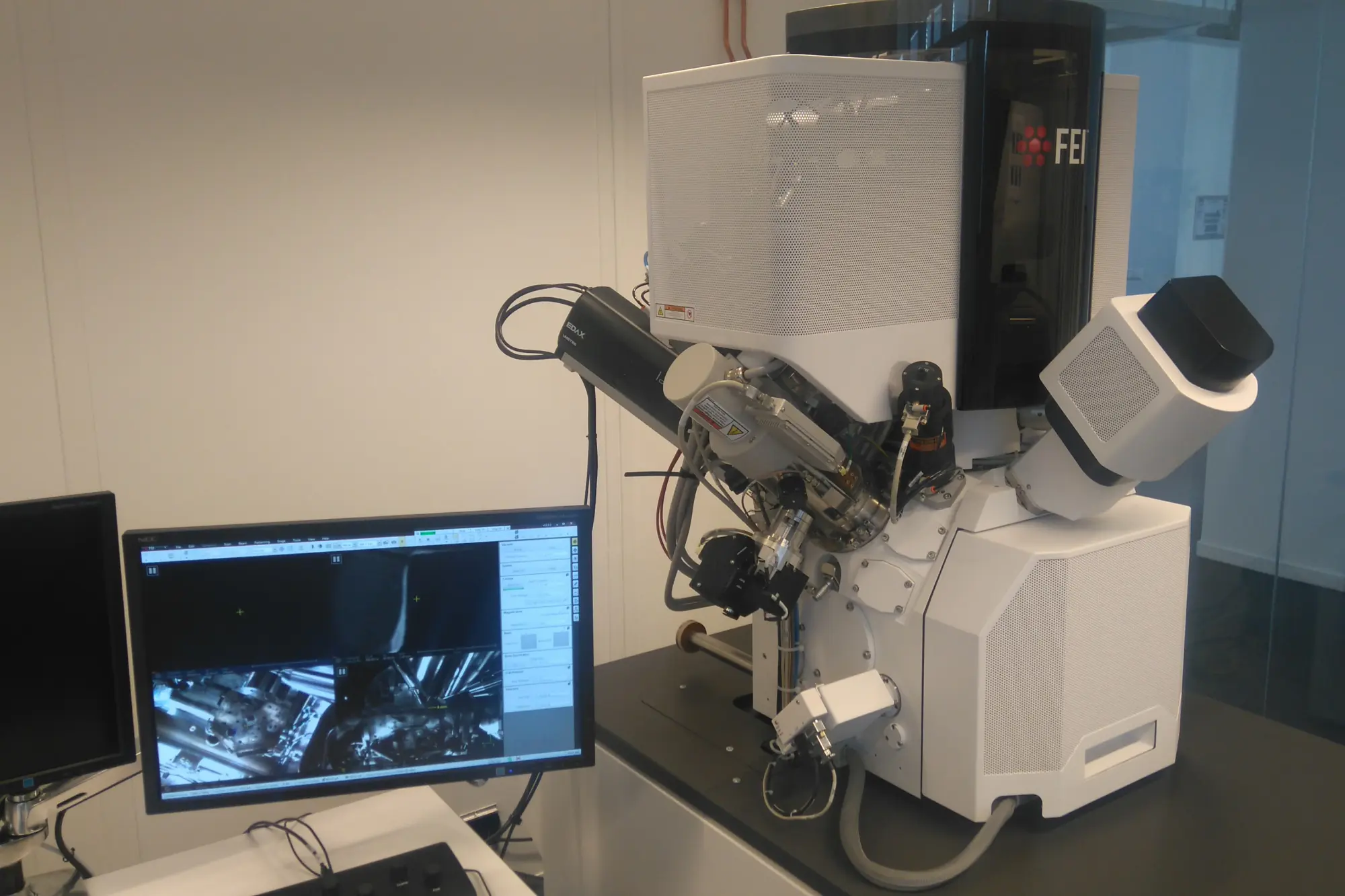
6- FEI FIBSEM Helios G4 CX (SEM and FIB): The tool offers high-resolution imaging and precise material removal for detailed sample preparation and analysis. Imaging, nanofabrication, TEM lamella preparation and 3D slice and view are among the typical functions of this tool. 

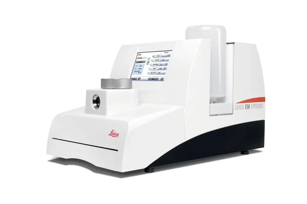
1- Leica CPD3 (critical point dryer): used for preparing delicate samples by removing liquid without causing damage. It employs a critical point drying process to transition samples from a liquid to a gas phase, preserving their structure and integrity. 

2- DISCO Dicer (dicing tool): a precision cutting tool used for slicing semiconductor wafers, crystals, and other materials into smaller pieces. It ensures accurate, clean cuts with minimal damage. 

3- EVG Bonder (wafer-to-wafer bonding tool): a tool for wafer bonding applications, including anodic, thermo-compression, and direct bonding. It is essential in the fabrication of microelectromechanical systems (MEMS), semiconductor devices, advanced materials research and packaging. 

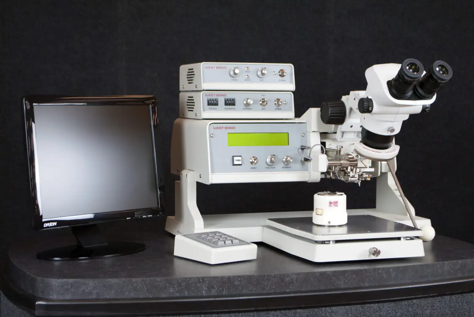
4- Westbond 4KE (wire bonder): a versatile wire bonder used for precise electrical connections in microelectronics and semiconductor devices. It supports both ball and wedge bonding, ensuring reliable and accurate wire placement. https://westbond.com/semi-automatic-wire-bonders/

Kavli nanolab:

Lorentzweg 1, 2628 CJ Delft

A virtual cleanroom tour is available here: